ASIC Turnkey Solution
End-to-end ASIC design services for IoT, from EDA to production-ready chips.
Complete ASIC Design Service for IoT
Arculus EDA UK offers a comprehensive ASIC Turnkey Solution that takes your product from concept to production. Our end-to-end service covers the entire semiconductor development pipeline, enabling you to focus on your core business whilst we handle the complexity of chip design and manufacturing.
Available on TSMC 12nm, 16nm, 22nm, and 40nm process nodes, our service is ideal for IoT applications requiring custom silicon solutions with optimised power, performance, and area.
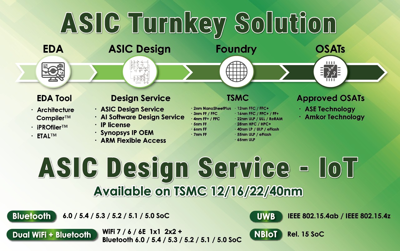
Our Design Pipeline
A streamlined four-stage process from design to delivery.
EDA
Electronic Design Automation tools and IP selection for your specific application requirements.
ASIC Design
Full SoC design service including architecture, RTL design, verification, and physical implementation.
Foundry
Tape-out and fabrication through our TSMC partnership, supporting 12nm, 16nm, 22nm, and 40nm process nodes.
OSATs
Outsourced Semiconductor Assembly and Test services to deliver production-ready packaged chips.
Supported Protocols
Our ASIC design service supports the latest wireless communication standards for IoT SoCs.
Bluetooth 6.0
Latest Bluetooth standard with enhanced range, speed, and positioning capabilities.
WiFi 7
IEEE 802.11be for ultra-high throughput and low-latency wireless connectivity.
UWB
Ultra-Wideband technology for precise indoor positioning and secure ranging.
NBIoT
Narrowband IoT for low-power wide-area network connectivity in IoT applications.
TSMC Advanced Process Nodes
Our ASIC design service leverages TSMC foundry capabilities across multiple process nodes, ensuring you get the optimal balance of performance, power efficiency, and cost for your IoT application.
Start Your ASIC Design Journey
Contact us to discuss your IoT SoC requirements and discover how our turnkey solution can bring your product to market faster.
Get in Touch